
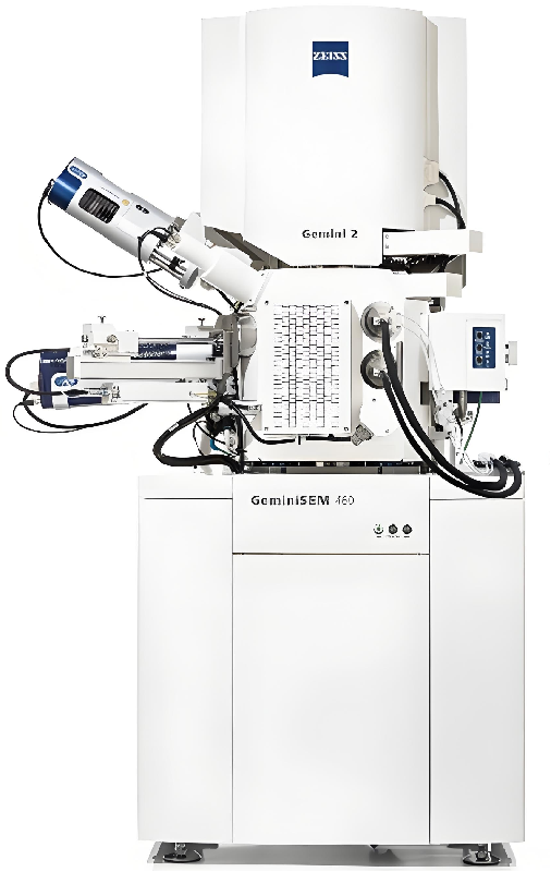
Brief description:A scanning electron microscope (SEM) is a way to observe things that falls between a transmission electron microscope and an optical microscope. It uses a tightly focused high-energy electron beam to scan a sample. Through the interaction between the beam and the material, various physical information is excited, which is then collected, amplified, and re-imaged to characterize the microscopic structure of the material. Modern SEMs can reach a resolution of 1nm, magnifications of up to 300,000 times or more that can be continuously adjusted, and they also have a large depth of field, wide view, and good 3D imaging effect. Additionally, when combined with other analytical instruments, SEMs can observe microscopic structures while also analyzing the composition of small areas of the material.
Industry Applications:Observation of material surface and cross-section morphology, analysis of elemental composition.


Detailed
A scanning electron microscope (SEM) is a way to observe things that falls between a transmission electron microscope and an optical microscope. It uses a tightly focused high-energy electron beam to scan a sample. Through the interaction between the beam and the material, various physical information is excited, which is then collected, amplified, and re-imaged to characterize the microscopic structure of the material. Modern SEMs can reach a resolution of 1nm, magnifications of up to 300,000 times or more that can be continuously adjusted, and they also have a large depth of field, wide view, and good 3D imaging effect. Additionally, when combined with other analytical instruments, SEMs can observe microscopic structures while also analyzing the composition of small areas of the material.
Product inquiry